
With the breakthrough of integrated circuit technology and the rise of the Internet of Things wave, MEMS (Micro Electro Mechanical Systems) technology has rapidly developed and become a key direction for national semiconductor research. Both the national "14th Five Year Plan" and Shenzhen's "14th Five Year Plan" have included the development of MEMS characteristic processes in their plans.
Recently, Shenzhen Business Daily launched a special report on "Strengthening the Leading Role, Remedying Shortcomings, Building Platforms, Expanding the Track | Anchoring the Semiconductor and Integrated Circuit Industry with" Strong Core Action ". Among them, Haipu Nano, as a representative enterprise, received an exclusive interview. The report focuses on the research and development path of nanoscale hyperspectral imaging MEMS technology, as well as the "four dimensional spatial perspective eye" of hyperspectral imaging in the fields of food safety, industrial testing, the Internet of Things, AR/VR, medical health, and other "super capabilities".
The following is the report content:
Taking a photo of an apple can quickly detect indicators such as sugar content, calories, moisture, softness, and hardness that cannot be seen by the naked eye. The behind the scenes contribution of having a pair of four-dimensional perspective eyes on the machine is hyperspectral imaging technology.
On June 15th, Huang Jinbiao, CEO of Shenzhen Haipu Nano Optics Technology Co., Ltd., showed reporters hyperspectral imaging MEMS (Micro Electro Mechanical Systems) with different wavelengths, which are similar in size to nail caps, to install the 'heart' for intelligent sensors that collect information.
By equipping them with different modules, a pair of perspective eyes can be installed on smart terminal devices, "said Huang Jinbiao.
The hyperspectral imaging sensor in Huang Jinbiao's hand belongs to MEMS sensors. The hyperspectral imaging technology behind it combines imaging technology with spectral technology, and by detecting one-dimensional spectral information and two-dimensional geometric spatial information of the target, unique "spectral patterns" of each object can be obtained. Based on the analysis of spectral information, hyperspectral technology can achieve direct detection of material components.
In response to the industry challenges of traditional hyperspectral cameras being bulky, expensive, and unable to be mass-produced, ocean spectroscopy nanooptics has been specifically designed to "gnaw" at the "hard core" of micro hyperspectral imaging MEMS sensors. At the beginning of its establishment in 2019, the first micro hyperspectral imaging MEMS technology was developed, designed, and fabricated. The following year, the second micro hyperspectral imaging MEMS sensor sample was successfully developed.
At the beginning of this year, Haipu Nano officially mass-produced the first generation of miniature hyperspectral imaging MEMS sensors, filling the gap in this field in China, and successfully developed a hyperspectral camera micro module with a volume of only one thousandth of that of traditional products. In May, Haipu Nano officially launched multiple products, including visible near-infrared hyperspectral industrial cameras, shortwave infrared hyperspectral industrial cameras, hyperspectral camera micro modules, and ultra-thin hyperspectral camera micro modules.
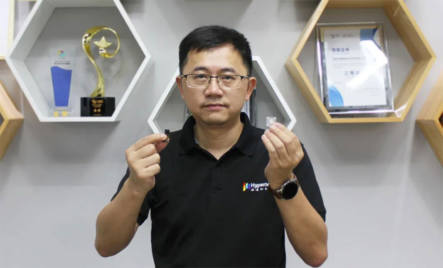
Huang Jinbiao showcases micro hyperspectral imaging MEMS and lens modules
Huang Jinbiao demonstrated to reporters the extraordinary capabilities of hyperspectral imaging technology in fields such as medical health, food safety, industrial visual inspection, environmental monitoring, Internet of Things, autonomous driving, AR/VR, etc.
Among them, hyperspectral imaging technology can accurately obtain information such as hemoglobin, melanin, oxygen content, and moisture in the skin, and timely detect skin health status. Based on hyperspectral information, hyperspectral imaging technology can accurately detect information such as pesticide residue content, sweetness, and moisture in fruits and vegetables. The hyperspectral environmental water quality monitoring camera and digital solution can achieve visual real-time tracking and detection of water quality.
Huang Jinbiao admits that MEMS sensors have personalized and decentralized characteristics, which are different from highly standardized integrated circuit chips in production processes. This non-standard feature is a soft spot that troubles the industry's rapid expansion.
But this also provides us with an opportunity to overtake on curves, "Huang Jinbiao believes. On the one hand, MEMS sensors have not yet formed a universal manufacturing process, and technology updates are slow, competing for skilled craftsmanship. On the other hand, product personalization brings vast segmented markets, making it difficult for a single company to achieve monopoly. China's rich market application scenarios can accelerate the 0-1-N process.
It is worth noting that in the key areas of key core technology research, the 14th Five Year Plan for National Economic and Social Development of Shenzhen and the Outline of Long Range Goals for 2035 also explicitly proposes to focus on technology research in the field of integrated circuits, focusing on chip architecture, developing characteristic processes such as insulated gate bipolar transistors and MEMS, and developing compound semiconductors such as silicon carbide.
This clearly gave Huang Jinbiao and his entrepreneurial partners stronger confidence.
 Tel : +86 18123751879
Monday to Friday:09:00-18:30
E-mail: Market@hypernano-optics.com
Address: 19th Floor, Building 1, COFCO Chuangxin R&D Center, Zone 69, Xingdong Community, Xin'an Street, Bao'an District, Shenzhen