
Recently, Shenzhen Haipu Nano Optics Technology Co., Ltd. (hereinafter referred to as "Haipu"), a leading global hyperspectral imaging enterprise, completed a round A financing of tens of millions of yuan. The investors in this round include Kunlun Capital, Yuanyuan Capital, and Wanxin Capital.
Innovate and strengthen China's "core", successfully mass produce Haipu micro hyperspectral MEMS chips
Shenzhen Haipu Nano Optics Technology Co., Ltd. was established in 2019, with its headquarters located in Shenzhen. With the mission of "spectral core vision, perception exceeding the limit", Haipu focuses on the design and research and development of hyperspectral imaging technology, breaking through the industry challenges of chip based, low-cost, engineering, and mass production of hyperspectral imaging MEMS. Its research and development capabilities cover the entire hyperspectral chain technology of chip design, optical modules, product cameras, algorithm applications, and can provide one-stop hyperspectral imaging solutions for customers in multiple fields worldwide.
Shenzhen Hypernano Optics Technology Co., Ltd
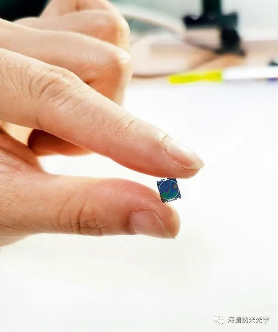
Haipu continues to focus on core technology research and development, miniaturizing hyperspectral cameras, and has become a global leader in the field of micro hyperspectral imaging. In response to the industry challenges of traditional hyperspectral cameras being bulky, expensive, and unable to be mass-produced, Hispectral specializes in the development of micro hyperspectral MEMS chips. In 2019, the first micro hyperspectral MEMS chip was developed, designed, and fabricated. In 2020, the second micro hyperspectral MEMS chip prototype was successfully developed, and the first generation of micro hyperspectral MEMS chips was officially mass-produced in early 2022, It fills the gap in this high-end and cutting-edge field in China and reaches the international leading level.
At the beginning of this year, Haipu successfully developed the industry's smallest hyperspectral imaging camera, which is only one thousandth the size of traditional hyperspectral cameras.
Chip-based Microminiaturization of Sea-spectrum Nanooptical Hyperspectral Imaging Published in Xinhua News Agency's "Outlook" Weekly
We do not confine our research and development achievements to laboratories, and Haipu actively cooperates with manufacturers and authoritative institutions such as medical, industrial, and consumer equipment to promote industrial upgrading.
In the medical field, the micro hyperspectral chips of Haipu can be combined with microscopes, and combined with spectral algorithms, precise cancer screening and diagnosis can be achieved.
In the field of water quality detection, the hyperspectral environmental water quality monitoring camera and digital solution of Haipu have achieved cloud image visualization of water quality tracking and real-time monitoring and reporting of water quality. The original "remote sensing" technology has become 24-hour * 7 all-weather "close sensing" monitoring.
Haipu also collaborates with major institutions both domestically and internationally to draft testing standards and methods for hyperspectral imaging technology in different fields, promoting the commercialization of hyperspectral technology.
The rapid development of Haipu is inseparable from the international research and development team behind it. The Haipu R&D team has nearly 20 years of design and manufacturing experience in the field of MEMS. The core members of the team include several top MEMS experts and peacock talents, with over 80% of personnel holding master's degrees or above. Since its establishment, Haipu has applied for a total of 59 invention patents, including 15 PCT international patents. Currently, Haipu's patent applications are still growing rapidly.
The billion level hyperspectral imaging market is about to explode, and Haipu is accelerating the construction of a hyperspectral imaging technology platform
Taking a photo can detect indicators such as sugar content, calories, and moisture in food; The factory inspection line is not afraid of environmental troubles such as light sources and colors. The camera can accurately detect product components without contact, with an accuracy rate of over one thousandth. The detection results of past minutes or hours can now be obtained in real-time online... Hyperspectral imaging technology can provide a pair of "golden eyes" for end devices, achieving the detection of everything, This revolutionary black technology is becoming an essential and fundamental common technology in the era of artificial intelligence.
Hyperspectral imaging technology can provide machine vision detection with
Fully automatic real-time online detection scheme
Hyperspectral imaging combines imaging technology with spectral technology, and by detecting one-dimensional spectral information and two-dimensional geometric space of targets, unique "spectral patterns" of each object can be obtained. Based on the analysis of spectral information, hyperspectral technology can achieve direct detection of material components, and its application scenarios include consumer electronics, industrial visual inspection, medical health, intelligent security, medical aesthetics, and many other fields.
From aviation remote sensing to machine vision, consumer equipment, and other industries, the hyperspectral imaging market is rapidly expanding in size. According to the "2021-2027 China's Hyperspectral Imaging System Industry Development Dynamics and Investment Direction Analysis Report" released by Zhiyan Consulting, the size of China's hyperspectral imaging market reached 6.895 billion yuan in 2019, and the overall market size has maintained a stable growth trend. It is expected that the market size will rapidly increase to 21.962 billion yuan by 2026.
As a leading enterprise in the field of hyperspectral imaging, Haipu will continue to increase investment in research and development and talent after the A-round financing, develop multiple products for different scenarios, achieve full spectrum coverage, accelerate the commercial implementation of hyperspectral imaging technology in many fields such as machine vision and consumer equipment, and continue to build a globally leading hyperspectral imaging technology platform, Provide hyperspectral imaging technology support for the industrial development of artificial intelligence and the upgrading of digital intelligence in various industries.
 Tel : +86 18123751879
Monday to Friday:09:00-18:30
E-mail: Market@hypernano-optics.com
Address: 19th Floor, Building 1, COFCO Chuangxin R&D Center, Zone 69, Xingdong Community, Xin'an Street, Bao'an District, Shenzhen